This thread will keep track of the first iteration of a custom power PCB for Project Quiver PT2. I will start with gathering the system requirements. For this I will look at Quiver PT1 and keep a record of the most important features and conditions.
Do you think splitting the one big connector into smaller connectors for each component/system and locating them according to their locations on the aircraft? i.e. locating the pixhawk connector on right/left side, altimeter on the other side, camera through the camera location, attachment interface connector at the back and so on. @Julius@errrks.eth
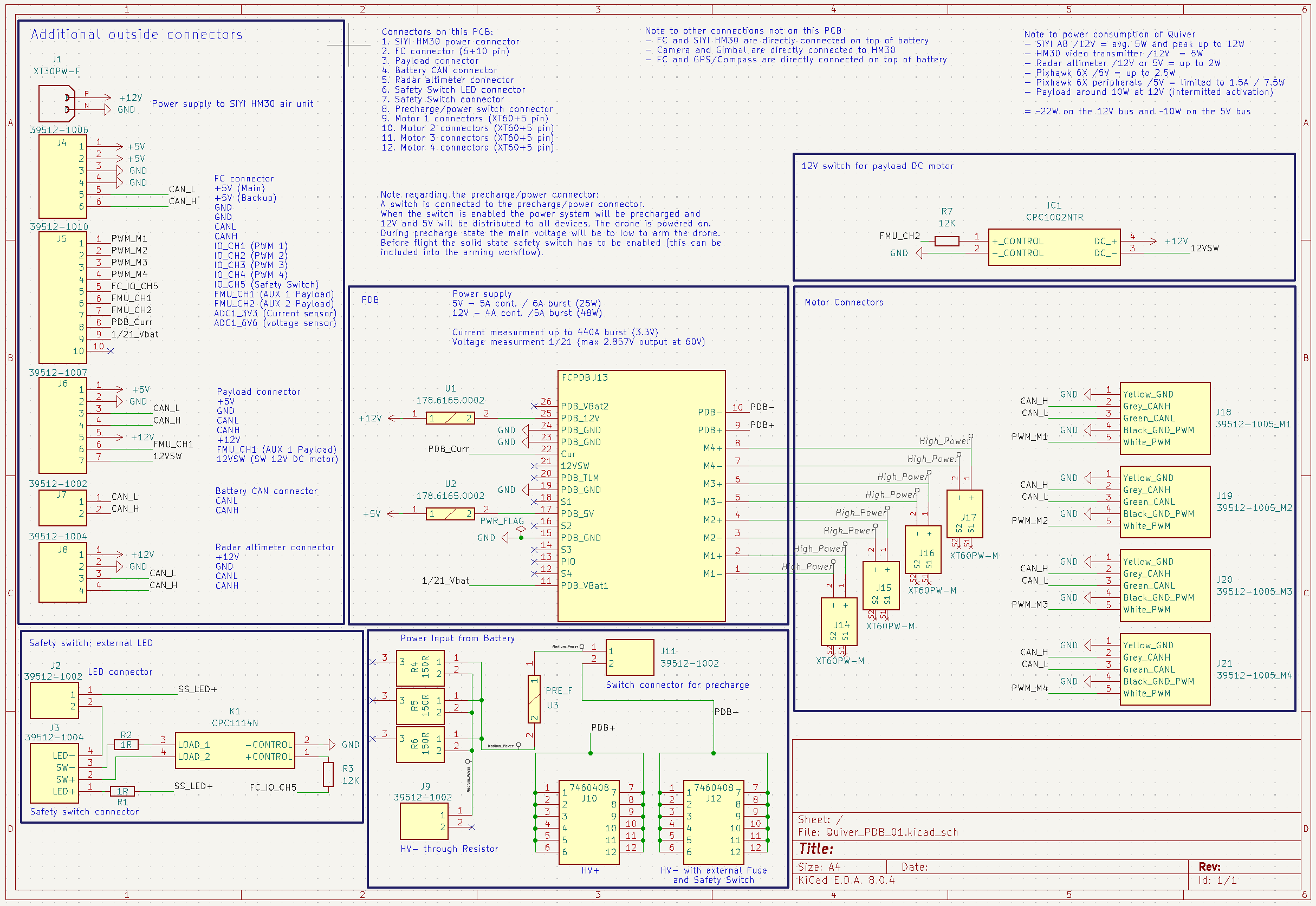
The PCB is not yet fully routed, but i added the high current lines to make it more visible how the main power is distributed. This is the top view on the PCB:
Thank you, Julius! This looks great and will be a much needed update for Quiver. I have reviewed the schematic and can’t think of any concerns or questions. The notes are very helpful.
Great Stuff, All looks good schematic wise, only comment would be when routing the PCB, dont skimp on distances between tracks at different potentials, and track widths, if possible consider adding a couple extra layers to separate HV and LV tracks.
I have a concern about the PDB voltage limit, the official document from Mateksys says the FCHUB 12S V2 PDB holds 8~60 voltage, but the main bus voltage from our fully charged Tattu 3.5 LiHV battery is 60.9.
Is that save for this design?
I don’t think thats an issue. If you run it on 70V then you might see a failure sooner (for example on a capacitor), but 0.9V more is to be neglected. Also it will only operate over 60V for <1% of its life. As soon as you run the motors the voltage will drop below 60V in seconds.